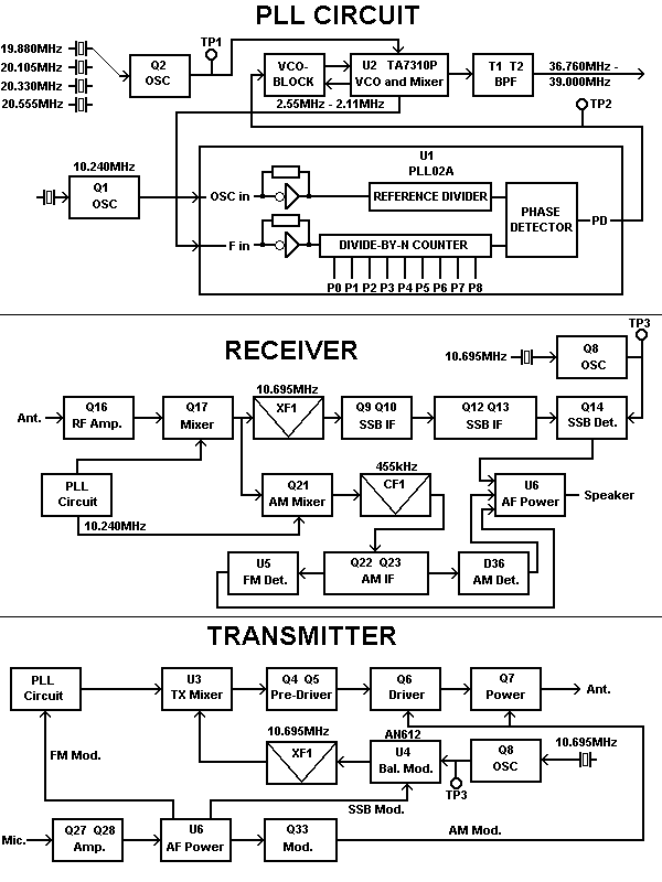
| Band | Ch. | FIN | P0 | P1 | P2 | P3 | P4 | P5 | P6 | P7 | P8 |
|---|---|---|---|---|---|---|---|---|---|---|---|
| 40 | 1 | 2.55MHz | 1 | 1 | 1 | 1 | 1 | 1 | X | X | X |
| 40 | 2 | 2.54MHz | 0 | 1 | 1 | 1 | 1 | 1 | X | X | X |
| 40 | 3 | 2.53MHz | 1 | 0 | 1 | 1 | 1 | 1 | X | X | X |
| 40 | 4 | 2.51MHz | 1 | 1 | 0 | 1 | 1 | 1 | X | X | X |
| 40 | 5 | 2.50MHz | 0 | 1 | 0 | 1 | 1 | 1 | X | X | X |
| - | |||||||||||
| 40 | 40 | 2.11MHz | 1 | 1 | 0 | 0 | 1 | 0 | X | X | X |
| - | |||||||||||
| -80 | X | X | X | X | X | X | X | X | 0 | 0 | 1 |
| -40 | X | X | X | X | X | X | X | X | 0 | 0 | 1 |
| 40 | X | X | X | X | X | X | X | X | 1 | 1 | 0 |
| 80 | X | X | X | X | X | X | X | X | 1 | 1 | 0 |
| 120 | X | X | X | X | X | X | X | X | 1 | 1 | 0 |
| Reading Point | Adjustment | Description | Value |
|---|---|---|---|
| PLL | |||
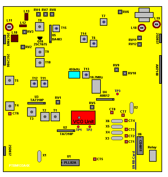
| TP2 | VCO-Block Coil | VCO Voltage | 4 Volt @ 27.185MHz |
| OSCILLATOR | |||
| U1 Pin 3 | Check | Reference Oscillator | 10.240MHz |
| TP1 | CT1 | RX AM -80 Band | 19.880MHz |
| TP1 | CT2 | RX AM 40 and -40 Band | 20.105MHz |
| TP1 | CT3 | RX AM 80 Band | 20.330MHz |
| TP1 | CT4 | RX AM 120 Band | 20.555MHz |
| TP1 | CT5 | RX LSB 40 Band | 20.1035MHz |
| TP3 | CT7 | TX AM | 10.695MHz |
| TP3 | CT8 | RX LSB | 10.692MHz |
| Adjustment | Description | Value | |
|---|---|---|---|
| RECEIVER | |||
| T8 | RF Input | ||
| T9 | RF Input | ||
| T10 | RF Input | ||
| T11 | 1. IF | 10,7MHz | |
| T12 | 1. IF | 10,7MHz | |
| T13 | AM IF | 455kHz | |
| T14 | AM Detector | 455kHz | |
| T6 | SSB IF | 455kHz | |
| T7 | SSB Detector | 455kHz | |
| T18 | FM Discriminator | 455kHz | |
| RV6 | SSB AGC | ||
| RV10 | Squelch | ||
| TRANSMITTER | |||
| T1 | PLL Output to Converter | 37.660 - 38.100MHz for CEPT | |
| T2 | PLL Output to Converter | 37.660 - 38.100MHz for CEPT | |
| T3 | Transmitter Output AM | 26.965 - 27.405MHz for CEPT | |
| T4 | Transmitter Output AM | 26.965 - 27.405MHz for CEPT | |
| T5 | Transmitter Output AM | 26.965 - 27.405MHz for CEPT | |
| CT6 | Transmitter Output USB/LSB | 26.965 - 27.405MHz for CEPT | |
| RV2 | Bias Q8 | ||
| RV11 | AM/FM Output Power | 10 Watt | |
| RV3 and RV9 | SSB Modulation | 18 Watt p-p | |
| RV1 | FM Modulation | +/- 2kHz | |
| RV12 | AM Modulation | 90% | |
| RV5 | Carrier at SSB | Adjust for minimum carrier leakage | |
| METER | |||
| RV4 | RF Power Meter | 10 Watt | |
| RV7 | RF S-Meter | SSB (USB/LSB) | |
| RV8 | RF S-Meter | AM/FM |
| Pin | Description |
|---|---|
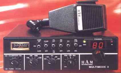
| 1 | Microphone |
| 2 | Ground |
| 3 | Speaker (Connect to Ground) |
| 4 | TX Key (Connect to Ground) |