| Reading Point | Condition | Adjustment | Procedure |
|---|
| PLL | | | |
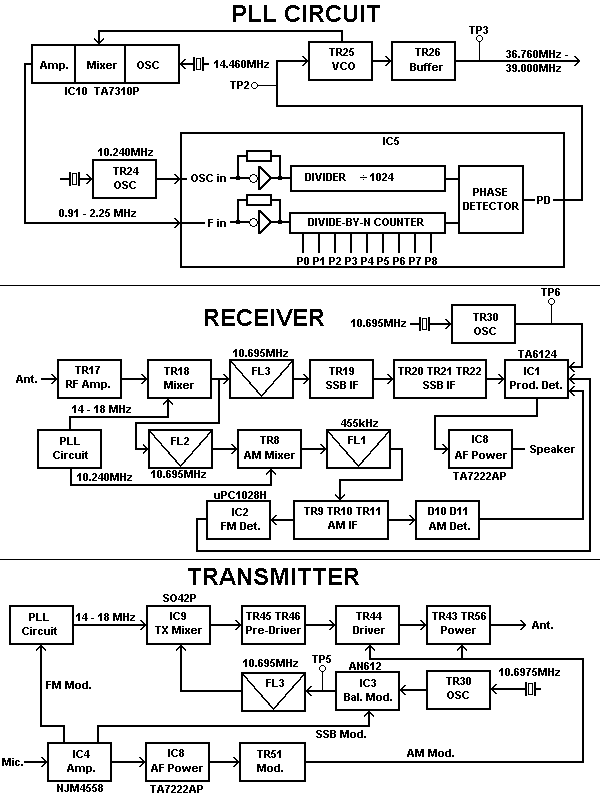
| IC5 Pin 3 | - | Check | 10.2400MHz |
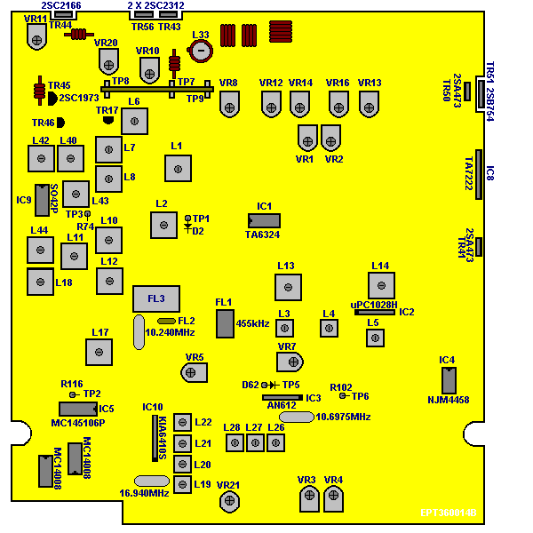
| TP2 | Band:D, Ch.:40 | L17 | 5,0 Volt |
| TP3 | - | L18 | Maximum on Oscilloscope |
| OSCILLATOR | | | |
| | | |
| 13.560MHz X-tal | | | |
| IC10 Pin 9 | AM | L19 | 16.0400MHz |
| IC10 Pin 9 | USB | L20 | 16.0425MHz |
| IC10 Pin 9 | LSB | L21 | 16.0375MHz |
| IC10 Pin 9 | TX AM | VR21 | 16.0400MHz (TX-Frequency) |
| 14.010MHz X-tal | | | |
| IC10 Pin 9 | AM | L19 | 16.4900MHz |
| IC10 Pin 9 | USB | L20 | 16.4925MHz |
| IC10 Pin 9 | LSB | L21 | 16.4875MHz |
| IC10 Pin 9 | TX AM | VR21 | 16.4900MHz (TX-Frequency) |
| 14.460MHz X-tal | | | |
| IC10 Pin 9 | AM | L19 | 16.9400MHz |
| IC10 Pin 9 | USB | L20 | 16.942525MHz |
| IC10 Pin 9 | LSB | L21 | 16.9375MHz |
| IC10 Pin 9 | TX AM | VR21 | 16.9400MHz (TX-Frequency) |
| All models: | | | |
| TP5 | TX AM | L26 | 10.6950MHz |
| TP6 | RX USB | L27 | 10.6925MHz |
| TP6 | RX LSB | L28 | 10.6975MHz |
| | | |
| TP5 | TX USB | VR7 | SSB Modulator Balance |
| | | |
| RECEIVER | | | |
| RX AM | L6 L7 L8 | RF Input |
| RX AM | L10 L11 L12 | AM/FM/SSB IF |
| RX AM | L3 L4 | AM/FM IF |
| RX FM | L5 | Discriminator Coil (FM Demodulator) |
| | | |
| | | |
| TP1 | RX USB | L1 L2 | Noise Blanker IF |
| | | |
| RX USB | VR3 | SSB Squelch |
| RX AM | VR4 | AM/FM Squelch |
| AM/FM S- Meter | RX AM | VR1 | |
| SSB S- Meter | RX SSB | VR2 | |
| TRANSMITTER | | | |
| TP9 (+) TP8 (-) | Bias Driver | VR11 | 10mA |
| TP9 (+) TP7 (-) | Bias Finale | VR10 | 100mA |
| TP9 (+) TP7 (-) | Bias Finale | VR20 | 100mA |
| TX AM | L42 | Maximum |
| TX AM | L43 | Mixer Coil (VCO-frequency input) |
| TX AM | L44 | Mixer Coil (TX-carrier 10.695MHz input) |
| TX AM | L40 L42 | Maximum RF output |
| TX AM | L33 | Minimum Harmonic |
| TX AM | VR13 | 15 Watt (30 Watt with Dual Finale output) AM/FM |
| TX USB | VR12 | 20 Watt (40 Watt with Dual Finale output) SSB (ALC) |
| TX AM | VR14 | 90% AM-Modulation (AMC) |
| TX FM | VR5 | 2 kHz FM-Deviation |
| TX CW | VR16 | CW Tone (Not in all model`s) |
| Power Meter | TX AM | VR8 | |
| | | |
| | | |
| | | |