
Cherokee CBS2100
CIRCUIT DESCRIPTION
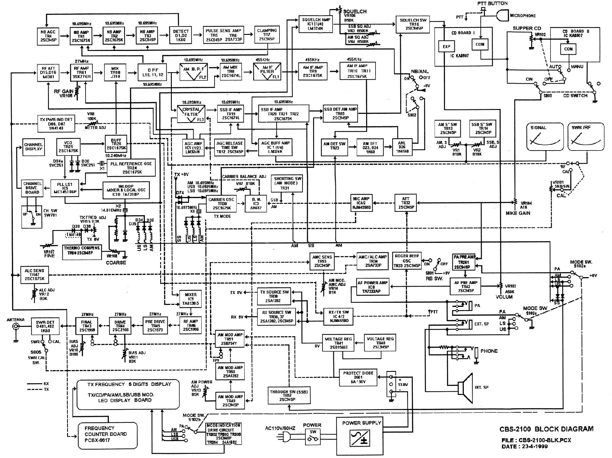
The CBS-2100 40 channels Citizen Band Base Station is constructed with a Phase Locked Loop frequency synthesizer to generate suitable RF signals for the double conversion receiver and the AM/SSB transmitter circuits. High level modulation is used in AM mode while low-level modulation is utilized in the SSB operation. A diode circuit performs AM detection and a transistor product detector demodulates the received SSB signal.
 Power Supplies Circuit
The CBS-2100 Base Station is designed to operation on AC as well as DC power sources.
When AC Power is used, the unit's internal AC power supply module will be used to convert 115VAC to 13.8V DC at the DC output plug. When AC is not available, just disconnect the DC output plug and replace it with an external 13.8V battery power source.
The output voltage of the AC power supply is fixed and there is no set up or adjustment points in the unit.
13.8V DC supplied from the DC Power connector at the back of the radio are protected against reversed connection by D93, and filtered by an AF choke T1. This supplies voltage directly to the audio power amplifier IC8, AM Modulator TR51 and the 8V regulator TR41.
Two transistor switches TR38 and TR37 turns on and off under the control of IC4 (pin7) to supply voltage to the transrnifter and receiver circuits. The Tx LED will grow in red on transmit.
Channel Selector
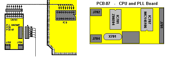
The channel selector circuit is divided into two parts. The pulsed rotary encoder switch SW701 with the LED display and its driver circuits in one board. The CPU IC701, PLL IC707 and its associated driver circuits are located in another PCB and they are molded in epoxy. Only 40 Citizen Band Channels are mask programmed into the CPU. No extra or spare leads on the CPU/PLL are accessible by the users.
When the channel switch (SW701) is turned clockwise, it sends a pulse to pin 3 or IC701. The CPU will find in its memory look-up table the correct PLL programmable divider division ratio and increment the channel number by 1, the action will revert to decrement when the channel switch is turned anti-clockwise. The data output are latched by IC704 and IC705 to drive the channel display LEDs, and latched by IC706 as the PLL division ratio for use by IC707.
Frequency Synthesizer
PLL is an abbreviation of the Phase-Locked-Loop. An MC45106 PLL integrated circuit, working together with a transistor Voltage Controlled Oscillator (VCO), a microprocessor controlled channel selector, and a down conversion mixer circuit TA-7310 to form a closed loop feedback circuit to generate suitable RF frequencies required for a 40 channel 27MHz CB operation.
TR24 is a Crystal Oscillator to generate the reference frequency of 10.24MHz. This signal is fed into IC707's reference frequency counter (pin 3) to obtain a phase comparison reference frequency of 10KHZ to its phase detector.
TR25 and Varicap Diodes D94 and D30 formed a Voltage Controlled Oscillator. The control voltage is obtained from the phase detector output of the PLL circuit to operate in a frequency range of 16.27 - 16.71 MHz. The output of the VCO is buffered by TR26 to fed the receiver and transmitter circuit.
IC10 TA7310P consists of an amplifier, an oscillator and a mixer. The oscillator is a crystal oscillator operated in a frequency trimmed by inductors and a varicap. Different inductors are connected into the oscillator circuit through switching diodes (D34 - D36) to provide different offset frequency settings in AM (14.010MHz), LSB (14.0075MHz) and USB (14.0125MHz). The output frequencies could be further trimmed by VR507 and varicap D124 for SSB Clarifier operation.
Part of the VCO output is coupled to the buffer amplifier in IC 10 (pin 7). It is then mixed with the 14.010MHz oscillator output to provide the PLL programmable divider input frequency of 2.26 - 2.70MHz at pin 6. The signal is fed to pin 2 of IC3 through a low pass filter circuit.
A microprocessor controlled channel switch circuit is employed to provide the division ratio to IC707 (pins 10 - 18) with correspondence to the channel number (1 - 40) selected by the user. The PLL input frequency (2.26 - 2.70MHz) is divided by the division ratio set by the channel selector to phase compare with the 10KHZ reference frequency. Any phase difference will result in a change of DC voltage output to the VCO. When the VCO frequency reaches the desired value, the DC output to the VCO stabilizes and the loop is in 'locked" condition.
The Lock Detector output (pin 8) of IC3 is used to inhibit the transmitter PTT and receiver audio circuits to ensure the radio always operate on the correct channel frequencies.
Both the PLL and CPU Integrated Circuits are molded in epoxy and are not serviceable by the users
10.695MHZ SECOND OFFSET OSCILLATOR
TR-30 is a crystal oscillator operates at a center frequency of 10.695MHz. The output of the circuit is trimmed by different inductors during AM, LSB and USB operation. On AM mode, D57 is biased on during transmit, and off while receiving. On USB or LSB mode D58 and D59 turns on respectively on Tx and Rx mode
This circuit provides 10.695MHz off-set frequency to L44 of the Tx mixer (IC9), which mixes with PLL VCO output to provide correct transmitting spot frequencies in AM operation. In SSB mode, D58 and D59 switches L27 and L28 into the circuit to provide canier signal of 10.6925MHz for USB and 10.6975MHz for LSB operation.
The signal is then routed to the Balanced Modulator (IC3) and Crystal Filter FL3 to generate low level SSB modulated signal for further processing by the Tx mixer (IC9). A portion of the signal is sent to the product detector (TR-15) for SSB demodulation.
FREQUENCY CALCULATIONS
The VCO frequency is obtained from the following calculation;
f vco = f off-set + Nfr
Where
f vco = VCO frequency.
N = Programming Code for divider output.
fr = Reference Frequency step, 10 KHz (0.01 MHz)
i.e. At channel #1 and AM mode, the corresponding N code is 226
f vco = 14.010 + 226 x 0.01 = 16.270 MHz
Since the mixer output determined by two factors: The second offset oscillator output (dependent on AM/SSB mode selector switch) and the PLL / VCO output.
Transmitter Operation
The VCO output is mixed with the second off-set oscillator signal and applied to the Tx mixer IC9 through band pass filters L43 and L44.
-For channel 1 AM mode, the output of Tx mixer is 16.270 + 10.695 MHz = 26.965 MHz (Ch 1 Tx frequency).
-For channel 1 LSS mode, the output of Tx mixer is 16.2675 + 10.6975 MHz = 26.965 MHz (Ch 1 LSB Carrier Frequency)
-For channel 1 USB mode, the output of Tx mixer is 16.2725 + 10.6925 MHz = 26.965 MHz (Ch 1 USB Carrier Frequency)
Receiver Operation
The output frequencies of PLL and offset oscillators remained the same for Rx operation.
For Channel 1 AM mode, the receiving frequency is 26.965 MHz
- Signal at 1st Local Oscillator Mixer is 26.965 - 16.270 MHz = 10.695 MHz (First IF)
- Signal at 2nd Local Oscillator Mixer is 10.695 - 10.240 MHz = 455 KHz (Second IF)
- Signal is detected by diodes at 455 KHz to recover audio
For channel 1 LSB mode, the receiving frequency is 26.964 MHz (using 1KHz modulating signal)
- Signal.at 1st Local Oscillator Mixer is 26.964 - 16.2675 MHz = 10.696.5 MHz (SSB IF)
- Signal at Product Defector is 10.6975 - 10.6965 MHz = I KHz (Audio)
For channel 1 USB mode, the receiving frequency is 26.966 MHz (using 1KHz modulating signal)
- Signal at 1st Local Oscillator Mixer is 26.966 - 16.2725 MHz = 10.693.5 MHz (SSB IF)
- Signal at Product Detector. is 10.6935 - 10.6925 MHz = 1KHz (Audio)
AM Modulation, Power Control and ALC
Input from the microphone is controlled by the Mic-Gain potentiometer VR505 and amplified by IC4. The amplified signal is used to drive the AM Modulator circuit consists of TR49 & 51.
There are two signals at the base of TR49, the DC voltage controlled by VR13 (RF Power Level Adjust), and the AF level from pin 1 of IC4. The DC bias controls the operating point of the Darlington pair transistors TR50 & 51 to provide power supply to the RF Power transistor's TR43 & 44, which controls the RF Carrier Power output of the radio. The AF signal is amplified and superimposed on the DC bias to create high level AM Modulation in TR43 & 44.
The maximum modulation is regulated by the Automatic Level Control (ALC) circuit consists of TR53, TR34 and TR32.
TR53 is a comparator circuit with set point adjusted by VR14. When TR53 conducts, the signal is half wave rectified by D83 to drive the current amplifier TR34, which in turn drives TR32 on and shunt down the Mic Audio signal at the input of IC4. The RC circuit (C135, R176 - 178) at the base of TR32 ensures the smooth operation of the ALC. When the modulator over modulates, AC voltages at emitter of TR53 will increase, and TR53 will conduct more during the negative cycle of the modulation signal, which increases the collector current of TR53 and turn TR43/TR32 on. The audio signal is shunted, input to the modulator decreases until it reaches the Modulation Limit set point of VR14.
SSB Modulation, Power Control and ALC
After being amplified by IC4, audio signals from the microphone are connected to the balanced modulator IC3 (pin 1). Signal from the second offset oscillator is presented to pin 3 of IC3 to produce the double side band suppressed carrier (DSBSC) signal. VR7 is adjusted for minimum carrier output.
The DSBSC signal is routed by the switching diodes to the 10.695MHz crystal filter, the unwanted sideband is filtered off, and the processed SSB signal is sent to L44/IC9 for mixing with the VCO output (at L43) to obtain the final transmitting frequency.
The high level modulator TR50 &51 are bypassed by TR52 during SSB operation. The RF Power amplifiers are biased to class B operation (VR10 -11) to preserve the envelope of the low-level modulated SSB signal. Since the SSB RF output is directly proportional to the level of audio signal driving the balanced modulator, the RF output is sampled by TR47, which provides negative feedback to the audio ALC circuit (TR34 & 53) to limit the rnaamurn SSB power output.
Receiver Circuits
RF signal from the antenna is coupled to the receiver circuit by C43, the signal passes through a pair of PIN fast switching diodes (D15/16), which are biased with AGC and a fixed voltages to protect the receiver front end from transmitter output and other excessively strong signals.
The signal is then amplified by a low noise MOSFET (TR51), passes a bandpass filter (L7 - L8) and mixed with the first local oscillator signal in TR18. The resultant first IF signal of 10.695MHz goes through a series of filter circuits, including those used for Noise Blanker operation, and come to the second mixer.
For AM operation, the IF signal is mixed with 10.240MHz second local oscillator frequency to product 455KHz second IF. The second IF signal is filtered and amplified by two stages of amplifiers (TR9, TR10 and 11), and then coupled to a diode detector (D23 & 24) for demodulation.
For SSS operation, the IF signal goes through the narrow band 10.695MHz crystal filter, amplified by two stages of IF amplifiers (TR19 - 22) and then coupled to a product detector (TR15) for demodulation.
The demodulated audio signal is amplified by TR15 and routed to the audio power amplifier IC8 via the volume control VR502. The audio amplifier is muted by voltages from D80 when Tx is active.
The output of AM and SSB IF amplifier's are also connected to an IC amplifier circuit (IC1) to provide Signal Meter DC voltages (pins 5 - 7), and the operation of Squelch Circuit (pins 8 - 10 & TR16). IC1 also provide AGC voltages (pins 1 - 3 & pins 12 - 14) to the receiver front end and the PIN protection diode D16.
The Noise Blanker taps noise signal from the first IF filter network (L10 - L12), amplify the signal by TR1 - TR3, demodulate it by D1 and D2. The detected noise level is further amplified by TR5 & TR6 to control TR7, which shunts the signal output level in the IF filter network (L12). The IF gain for the noise signal is therefore reduced.
Transmitter Circuit
The RF signals generated from the PLL and the second offset oscillator / balanced mixer are assembled at RF Mixer IC9 to provide the final transmitting signal. The signal passes through a bandpass filter (L40 & 42) to two stages of RF pre-driver's (TR45 & 46), RF driver TR44, the final stage amplifier TR43, a low pass filter network and then to the antenna.
In AM operation, modulated voltages only applies to the collectors of TR43 and TR44, while SSB signals passes through all of the RF amplifier chain (TR43 - 46). Please refer to the previous sections for detail description of frequency generation and modulation.
The output signal is picked up by D86 & D87 to give relative RF output power meter indication, and a Standing Wave Ratio (SWR) sampling circuit consists of D401 and D402 provides the SWR meter indication feature.
"Clear Drive" Compander Circuit
The CBS-2100 radio is equipped with a compander circuit, which will be marketed under the trademark of "Clear Drive". The feature could be enabled or turned off by a front panel switch labeled as 'CDS'
The Compander circuit consists of IC901 is employed. The circuit can be divided into three parts:
Compressor
Low Pass Audio Filter
Expander
Transmit audio from the microphone is routed to pin 8 of IC901for amplification, and then to the internal Compressor circuit for audio processing. Output from the Compressor (pin 3) is routed through an active three pole low pass filter (pins 1& 2) to the Mic Gain control. All the excessive high frequency signals are suppressed by the filter before transmission.
The reference level of the Compressor is set by R905 to around 5mV microphone input. R901 is inserted into the circuit to obtain suitable modulation level. Received audio from the detector is sent to pin 15 for amplification, and then to the internal Expander circuit for audio processing. The reference level is set by R908 to around 12dB SINAD, the output is taken from pin 19 and is connected to the Volume control on the front panel.
Pin 12 of IC901 provides the bypass feature. When a high level is present, both the Compressor and the Expander are operative. When pin 12 is connected to ground potential, both the Compressor and the Expander are bypassed - All the audio level passes through IC901 without getting any level processing.
In order to increase the dramatic effects of Clear Drive on transmit, CBS-2100 is equipped with dual stage Clear Drive configuration called Super CDS, The user could activate Super CDS by turning VR102 from OFF position clockwise (Auto-CDS) to adjust the compression ratio of the compander. When VR102 is at OFF position, the Clear Drive internal circuits automatically fix the compression ratio. Super CDS is a transmit audio enhancement circuit and has no effects over CDS for the receiver circuit.
Frequency Counter Circuit
A frequency counter is included in the CBS-2100 to facilitate the Single Side Band operation. The counter is built around a mask programmed Z80 type CPU.
The frequency generated by the PLL synthesizer is taped from the 10.695MHz offset frequency generator IC10 through L22. The signal, which is 10.695MHz below the TX or the RX operating frequencies is fed to IC603 - a divided by 40 prescaler system to match the lower frequency counting rate that the CPU is operating on.
In additional to the frequency counting application program, there is a look up table in the internal masked memory of the CPU to add 10.695MHz back to the counted frequency so that the correct 27MHz frequencies could be displayed.
The CPU output is sent to a demuliplexer/driver combination of IC604 and IC601 to display the frequency information on a 6 digit 7 segment LED display on the front panel.
There is no internal set up or adjustment required for this frequency counter.