![]()
![]()
 Fundamental theory of PLL circuit
The word PLL is an abbreciation of the "Phase Locked Loop" in which a given
signal is processed to track the frequency and phase of a reference signal.
In other word, the PLL is of an automatic frequency control loop or automatic phase
control.
The PLL circuit consists of the three units in simple form as shown:
 In the above block diagram, when the reference frequency fr and the
VCO output frequency fv to be compared are applied to the Phase Detector P/D, fv is
compared with fr in terms of Phase lag and lead.
In the above block diagram, when the reference frequency fr and the
VCO output frequency fv to be compared are applied to the Phase Detector P/D, fv is
compared with fr in terms of Phase lag and lead.
Then the resulting output (Phase difference) is converted in to the DC output voltage
corresponding to the phase difference. Since the phase comparison is made at every cycle ,
the DC output may include unnecessary harmonics and noises . The DC output is , then, led
to the low pass filter ( L.P.F) and integrated or smoothed to continuous DC voltage in
proportion to the phase difference. The frequency of voltage controlled oscillator
(V.C.O.) is controlled by the L.P.F. output voltage. Thus, controled VCO output is, then,
split into two:
One used as an operating frequency of the unit and another will be returned to the plD,
making a closed loop. The closed loop will con tinue to operate untill the following
condition is met :
�r(t) = �o(t)
This condition is called locked.
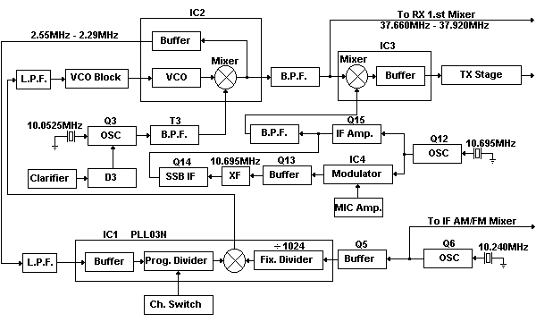
Employing the PLL system into a CB transciever requires some modifications so that the VCO
generates specific frequency corresponding to each channel frequency [1 - 22 ] according
to the channel selection. In the diagram below, a programmable divider, Mixer and Offset
oscillator are newly added. 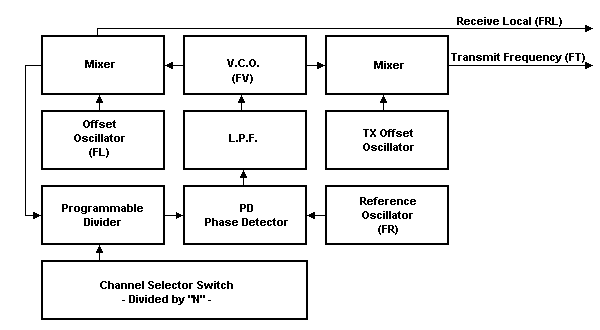 Q6 is the standard reference oscillator
(lO.24OMHz) and Q5 is the buffer amp-lifier for the oscillator.
Q6 is the standard reference oscillator
(lO.24OMHz) and Q5 is the buffer amp-lifier for the oscillator.
D6 is the diode through which DC voltage , which is supplied when the channel selector is
placed between channels , is applied to the IC3 to disable the mixing operation inside the
IC3. Thus no frequency will be generated though the channel selector is placed between
correct channel positions.
For clearer understanding, please refer to the schematic diagram and the Block Diagram.
AM/FM receiver circuit
A received signal passes T7 , then amplified in Q2O, and again passes the band pass filter
consisting of T8 and T9, then, enters into the Mixer stage of Q22. On the other hand the
first Rx local signal frequency is applied to the base of Q22 through a coupling capacitor
of C14. Then, both signals are mixed with inside the Q22 and converted into the first IF
signal (10.695MHz) in passing through the T10 and T13. The 10.695MHz signal and 10.240MHz
signal generated in Q6 are applied to the balanced mixer consisting of D22 and D23 and
455kHz second IF frequency will be made .
This frequency is then led to the T14, CF (ceramic filter), Q27, Q28, Q29 (amplidied), T15
and finally led to the detector D25. The audio signal is then applied to the AF amplifier
(IC5) through ANL CD26) circuit. The IC output drives the built-in speaker.
To improve signal over load distortion which would be caused when the receiver is
subjected to a strong signal, three stages of AGC loops., each for Q20, Q22 and Q27, are
provided.
Q21 is a switching transistor to short-circuit the primary circuit of T9 during transmit
operation , thus disabling the receiver circuit.
While in FM receiving mode, the 455kHz signal amplified only through Q27 is led to FM
demodulating IC, IC5O1 through T16. Resultant demodulated audio is acheived from the 1C
pin #12 and input to AF gain control VR, VR1.
SSB receiver circuit
An incoming signal induced on the antenna is led to the T7 and applied to the then to Q20
and amplified. The amplified output is applied to the Q22 mixer through a bandpass filter
consisting of T8 and T9. While the first local frequency is being applied to the base of
the same transistor, both frequencies are mixed with each other and first IF frequency
will be made (10.695MHz for AM/FM/USB , 10.692MHz for LSB) . This IF signal then amplified
in passing through the T10, crystal filter, Q14, Tll, Q16 and Q17 and finally detected
into the audio signalwith the product detector consisting of Q19. The audio signal is led
to the Power IC (IC5) to drive the built-in speaker.
Q18 is the transistor to avoid undesirable impule noise , which will be generated in
pressing the push-to-talk switch, from entering into the AGC circuit.
. To reduce the signal over load distortion in the SSB mode of operation, peak-value type
AGC circuit consisting of Q3O, and Q31 is employed for exclusive use of SSB operation.
AM/FM transmitter circuit
The first local oscillator frequency (37MHz band) and 10.695MHz frequency generated in the
Q12 are led to the Pin #4 and Pin #1 of IC3, respectively, and mixed with each other,
resulting in 27MHz band transmit frequency . The 27MHz output is led to the Q8, Q9, and
Q10 through T4 and T5 in this order and amplified up to the high level necessary for
transmission.
Thus amplified Power output is applied to the Antenna Connector through a bandpass filter
consisting of L11, L12, L13, etc.
0n the other hand, the microphone input signal enters into the Power IC,(IC5, #6Pin
terminal) and amplified output is applied to the collectors of Q9 and Q10 through the
trans former T16 and diode D43 to modulate the transmit carrier frequency .
Transistor Q35 is the automatic level controller provided to suppress the audio input
level to the IC5 properly to avoid the over modulation.
Q37 obtains its input signal from the audio output circuit through D43 and its output
controls Q35, thus keeping modulation signal level to a relatively cons tant value.
In the FM mode, IC5 output is fed to the anode of the variable capacitor D4 in IC2 VC0
circuit, varying its bias to change VC0 signal phase component, finally giving deviation
to PLL output frequency.
SSB transmitter circuit
In the mode of SSB operation, either of first local oscillator frequency of 37.660 -
37.920MHz (AM/FM/USB) or 37.657 - 37.917MHz (LSB) will be led to the IC #4Pin terminal. On
the other hand the 10.695MHz (in LSB mode, this will be shifted to 10.692MHz as previously
mentioned) generated with Q12 is led to the balanced modulation IC (IC4) . The 1C is
designed to produce carrier-suppressed double side band signals when an audio signal
amplified with IC5 is applied .to the PIN terminal of #1. Thus produced DSB signal will
flow to Q13 and amplified , then led to the XF(crystal filter) to separate the desired
side band.
The side band signal is led to the Q14 and be amplified, then led #3Pin terminal of IC3
and mixed with the output is led to the the first local signal to oscillator produce 27MHz
transmit signal. The 27MHz SSB output is the led to the T4 and T5, then further led to the
linear amplifiers, Q7, Q8, Q9 and Q10.
Thus amplified RF output is finally led to the antenna terminal through the Bandpass and
low pass networks provided between the Q10 and antenna connector.
To avoid over modulation distortion , an ALC circuit consis ting of Q35 and Q38 is
provided in the SSB microphone amplifier circuit. Another ALC circuit is also employed in
the RF circuit (from Q10 to IF Amp Q14) to reduce the distortion in the RF stages.
Transistor Q36 and Q39 are switching circuits to operate IC5 as an SSB microphone
amplifier.
Noise blanker circuit
An impulse signal included in the IF signals will be picked up through the capacitor C113
and positive-half voltage is then applied to the transistor Q24 and Q25 and amplified to
enough level capable of turning the transistor Q26. The amplified impulse signal makes Q26
turn on while the impulse is being applied. In other word, the primary circuit of T10 is
grounded to the chassis through C121 and the emitter- collector of Q26, so no mixer output
will be obtained during this period. In this way the impulse noise will be blanked out.
D20 is the diode provided to control the bias voltage to the Q24 in according to the
signal strength of the normal signals recieved, thus avoiding operation error which would
caused by the normal signals.
Squelch circuit
When AGC voltage lowers with a weak recieved signal, transistors Q32 and Q33 turn on and
this makes Q34 turn off, controlling the bias voltage to the AF AMP (IC 5) and disabling
the amplifier. On the other hand when the transistor Q34 is turned on, the amplifier will
start to operate.
Regulated power supply circuit
This circuit consists of Q44 and D50 and supplies voltage through the switching
transistors Q40, Q41, Q43, depending upon the mode of operation.
Test equipment required:
| Power Supply: 13,8 V | Frequency Counter | Dummy Load 50 ohm | Oscilloscope |
| DC Amperemeter | RF SSG | AF SSG |
Preparation alignment:
| Clarifier | Mid. |
| SQ GAIN | Max. |
| AF GAIN | Max. |
| RF GAIN | Max. |
| MIC GAIN | Max. |
| MOD, S/RF | S/RF |
| NB/ANL | Off |
| Band | D |
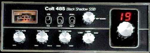
| Channel | 19 |
| Step | Adjust | Indicator Connection | remarks |
|---|---|---|---|
| PLL | |||
| 1 | CT3 | Frequency Counter to TP2 AM-Modulation |
10.240MHz |
| 2 | CT1 | Oscilloscope and Frequency counter to TP3 AM-Modulation |
20.105MHz |
| 3 | CT2 | Frequency Counter to TP2 LSB-Modulation |
20.1035MHz |
| 4 | CT5 | Frequency Counter to TP5 AM-Modulation |
10.695MHz |
| 5 | CT4 | Frequency Counter to TP5 AM-Modulation |
10.692MHz |
| VCO | |||
| 6 | VCO-Block | Volt Meter to TP1 | 4,4Volt@Channel 19 |
| RF Amplifier Bias Alignment | |||
| 7 | RV1 | VoltMeter between Q10 Emitter and GND | 35mA |
| SSB Power Amplifier stage Alignment Channel 11 |
|||
| 8 | T1 | Oscilloscope and Watt Meter to Antenna jack | Feed 2,4kHz to Microphone input. Adjust for maximum amplitude. |
| 9 | T2 | Oscilloscope and Watt Meter to Antenna jack | Feed 2,4kHz to Microphone input. Adjust for maximum amplitude. |
| SSB Power Amplifier stage Alignment | |||
| 10 | T4 | Oscilloscope to base of Q8 Channel 22 |
Feed 2,4kHz to Microphone input. Adjust for maximum amplitude. |
| 11 | T5 | Oscilloscope to base of Q8 Channel 1 |
Feed 2,4kHz to Microphone input. Adjust for maximum amplitude. |
| SSB Power Amplifier stage Alignment Channel 11 |
|||
| 12 | T6 | Oscilloscope to emitter of Q7 | Feed 2,4kHz to Microphone input. Adjust for maximum amplitude. |
| 13 | T11 | Oscilloscope and Watt Meter to Antenna jack | Feed 2,4kHz to Microphone input. Adjust for maximum amplitude. |
| 14 | L7 | Oscilloscope and Watt Meter to Antenna jack | Adjust for maximum |
| 15 | L11 | Oscilloscope and Watt Meter to Antenna jack | Adjust for maximum |
| 16 | L13 | Oscilloscope and Watt Meter to Antenna jack | Adjust for maximum |
| 17 | RV4 | Oscilloscope and Watt Meter to Antenna jack | Adjust for minimum Carrier lekage |
| 18 | RV5 | Oscilloscope and Watt Meter to Antenna jack | Adjust for minimum Carrier lekage |
| 19 | RV11 (ALC) | Oscilloscope and Watt Meter to Antenna jack | Feed 500Hz and 2,4kHz to Microphone input. Adjust for 18 Watt. |
| AM Power Alignment | |||
| 20 | RV1 | Oscilloscope and Watt Meter to Antenna jack | Adjust for 12 Watt RF Power |
| Modulation Alignment | |||
| 21 | RV12 | Oscilloscope and Watt Meter to Antenna jack | Adjust for 80% AM-modulation |
| RF Power Meter Alignment | |||
| 22 | RV3 | Watt Meter to Antenna jack | Adjust RF Power Meter |
| Lock Out Circuit Check | |||
| 23 | - | VoltMeter between base of Q9 and GND | 0,05 - 0,4 Volt |
| Transmit Frequency Check | |||
| 24 | - | Frequency Counter to Antenna jack | Read fequency on each channel (+/-900Hz) |
| RECEIVER | |||
| AGC Alignment | |||
| 25 | RV8 | VoltMeter to Terminal 15 on PCB and GND | Adjust for 2 Volt |
| Receiver Sensitivity Alignment (AM-Mode) | T7 | 8 ohm Dummy Load and Oscilloscope to external Speaker jack | Adjust for maximum |
| 26 | |||
| Squelch Sircuit Alignment | |||
| 27 | RV9 | 8 ohm Dummy Load and Oscilloscope to external Speaker jack | Adjust so that the Audio output just appears on the Oscilloscope |
| 28 | RV10 | 8 ohm Dummy Load and Oscilloscope to external Speaker jack USB-Modulation |
Adjust so that the Audio output just appears on the Oscilloscope |
| S-meter Alignment | |||
| 29 | RV7 | 8 ohm Dummy Load and Oscilloscope to external Speaker jack | SSB-Modulation. RF SSG and Ajust for "S" = "9" |
| 30 | RV6 | 8 ohm Dummy Load and Oscilloscope to external Speaker jack | AM-modulation. RF SSG and Ajust for "S" = "9" |
| FM Modulation Alignment | |||
| 31 | RV501 | Connect Diviation Meter to Antenna jack. | Adjust for 1,5kHz Modulation |
| Pin | Description |
|---|---|
| 1 | Microphone |
| 2 | Ground |
| 3 | Speaker (Connect to Ground) |
| 4 | TX Key (Connect to Ground) |
PTBM048A0X Schematic Diagram
PLL02N PLL Frequency Synthesizer
PLL03N PLL Frequency Synthesizer
AN240P FM IF Amplifier and Detector
Quieting of AM reception and improving gain of incoming signals is a common request
from radio operators. In the first stages of the HF input 2SC710 transistor can be found.
This transistor is responsible for the amplification of a small detected signals. A
problems exist if the transistor itself is noisy as is such the case of the 2SC710 when
compared to other low noise packages. Along with the amplification of the incoming signals
is transistor noise. Replacement of this transistor with a higher gain, lower noise
transistor greatly improves the signal to noise ratio of your receiver.
We will use an 2SC2999 transistor that has higher gain lower noise characteristic. Replace
the 2SC710 (Q20) with an 2SC2999 (or similar low noise
and high gain transistor) to achieve this improved signal to noise ratio.
Re-Adjust T7 and T8
The gain will improved with more than 6dB with the same signal to noise ratio.