| Power Supply: 13,8 V | Frequency Counter | Dummy Load 50 ohm | Oscilloscope |
| DC Amperemeter | RF SSG | AF SSG |
| Clarifier | Mid. |
| SQ GAIN | Max. |
| AF GAIN | Max. |
| RF GAIN | Max. |
| MIC GAIN | Max. |
| MOD, S/RF | S/RF |
| NB/ANL | Off |
| Reading Point | Condition | Adjustment | Procedure |
|---|---|---|---|
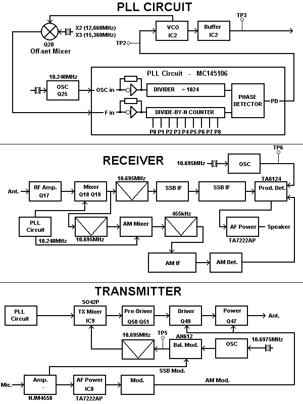
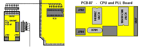
| PLL | |||
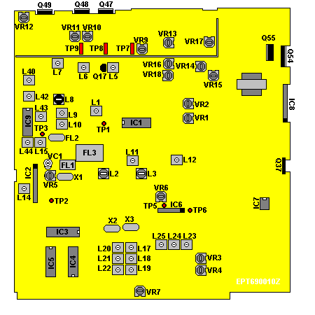
| Vonnect Voltmeter to TP2. Connect Oscilloscope to TP3. | G-band Ch. 40 AM RX-mode | L14 L15 | 6,5V +/- 0,1V |
| Connect FrequencyCounter to TP5. | G-band Ch. 1 AM RX-mode | L23 | 10,695MHz +/- 20Hz |
| OSCILLATOR | |||
| Connex CX4400: | |||
| Connect FrequencyCounter to TP3. | G-band Ch. 40 AM RX-mode | L17 | 18,890MHz +/- 20Hz |
| Connect FrequencyCounter to TP3. | E-band Ch. 1 AM RX-mode | L20 | 17,550MHz +/- 20Hz |
| Connect FrequencyCounter to TP3. | G-band Ch. 1 AM TX-mode | L20 | 18,890MHz +/- 20Hz |
| RECEIVER | |||
| RF SSG to antenna jack. 28,915MHz 1uV output 30% modulation | F-band Ch. 19 RX AM-mode | L2, L3, L4, L5, L6, L7, L8, L9, L10 | Maximum at audio output |
| RF SSG to antenna jack. 28,245MHz 1uV output 30% modulation | B-band Ch. 1 RX AM-mode | L5, L6, | Maximum at audio output |
| RF SSG to antenna jack. 29,585MHz 1uV output 30% modulation | G-band Ch. 40 RX AM-mode | L5, L6, | Maximum at audio output |
| RF SSG to antenna jack. 28,915MHz 100uV output 3kHz deviation | F-band Ch. 19 RX FM-mode | L4 | Maximum at audio output |
| RF SSG to antenna jack. 28,915MHz 0,5uV output Modluation off Connect Voltmeter to TP3 | F-band Ch. 19 RX AM-mode NB-ANL ON | L1 | DC voltage to maximum |
| RF SSG to antenna jack. 28,915MHz 0,5uV output 30% modulation | F-band Ch. 19 RX AM-mode NB-ANL ON | VR3 | Adjust until squelch just open |
| RF SSG to antenna jack. 28,915MHz 0,5uV output 30% modulation | F-band Ch. 19 RX AM-mode | VR1 | Adjust internal meter to "S9" |
| TRANSMITTER | |||
| Connect RF-Power meter to antenna jack | F-Band Ch. 19. AM TX-mode | L40, L42, L43, L44 | Maximum power |
| Connect RF-Power meter to antenna jack | F-band Ch. 19 AM TX-mode | VR9 | RF Power meter |
| Connect Oscilloscope to antenna jack | F-band Ch. 19 AM TX-mode | VR16 | 95% AM-modulation |
| Connect Deviation meter to antenna jack | F-band Ch. 19 FM TX-mode | VR5 | 4kHz FM Deviation |
| Connect RF-Power meter to antenna jack | F-band Ch. 19 | VR14 VR18 | High power Low power |
| Pin | Description |
|---|---|
| 1 | Ground |
| 2 | Microphone |
| 3 | TX Key (Connect to Ground) |
| 4 | Speaker (Connect to Ground) |